VDMA Productronics Special Exhibit

In cooperation with the specialist department VDMA Productronics, the conceptual and technical sponsor of productronica, the special show presents eight exhibitors who will provide information through live demonstrations on topics such as chip development, systems for electric aircraft, superconductors, the “Microtec Academy,” the “PhoenixD Cluster of Excellence,” advanced packaging, power electronics, and much more.
Hall B2, Booth 461
Chipdesign Germany
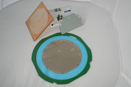
At the Chipdesign Germany booth, visitors will gain insight into the German network for chip development. They can follow the development process of digital integrated circuits — from initial idea to design to finished hardware. Exhibits, such as wafers, masks, and chips, will illustrate the individual steps and can be viewed directly under a digital microscope.
Additionally, the Chipdesign Germany network will present itself. The network connects research institutes, companies, and funding initiatives that collaborate on open tool chains, innovative designs, and new training concepts. This demonstrates how Germany is expanding its expertise in chip design and contributing to technological sovereignty.
The exhibition area clearly shows how digital integrated circuits are created, from initial conception to finished product. Using real exhibits, such as wafers, masks, and chips, visitors can observe the development process and view the structures live under a high-resolution digital microscope. This "look inside" is a special highlight of the exhibition, making chip design tangible and experiential.
The presentation is supplemented by information on the "Chip Design Germany" network. This network brings together research, industry, and education to develop joint solutions for open tools, new training concepts, and innovative chip architectures. This makes the process understandable and highlights Germany's role in strengthening European semiconductor expertise.
The special exhibition is intended for trade visitors from industry, research, and education who wish to learn about modern chip development.
It is particularly appealing to developers, students, company representatives, and decision-makers in chip design, mechanical engineering, and plant construction interested in new tools, processes, and collaborations.
Beginners will also find it an accessible introduction to the methods and results of circuit development.
Elektra Solar
On display is the two-seater Elektra Trainer, an ultralight electric aircraft. Certified in the German ultralight class, it has a flight time of over two hours.
Manufacturers of battery systems, electric motors, electronics, and solar systems will learn how their products could power tomorrow's solutions.
SupraMotion—Superconductors in industrial automation
Superconductors have great potential for use in the industry of the future. They enable contactless storage and movement of objects with low energy consumption and without any control technology. Since they operate without dust or abrasion, they are ideal for transporting objects in a protected manner in very clean environments. They can even be manipulated through walls.
Superconductors are materials with unique magnetic properties: when cooled below a certain temperature, they can anchor the field of a permanent magnet inside them. This creates a strong yet invisible coupling. This keeps the magnet and superconductor at a defined distance from each other – even through walls, in liquids, or in a vacuum. As long as the superconductor remains below its transition temperature, it stores the "fingerprint" of the magnet in its magnetic memory, thus retaining its position. This information is retained even when the two are separated.
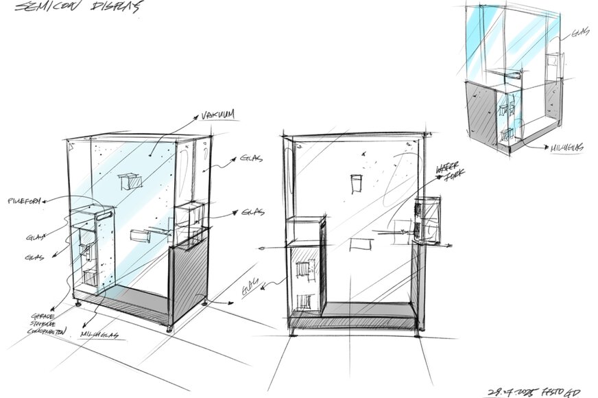
Our demonstrator shows an optimized, scaled-down EFEM process for easy handling of 8-inch wafers in a pallet-compatible size. A SMIF system is used instead of FOUPs. Technical highlights include contactless wafer handling with SupraMotion, gate control via the new VESC, and a PinLifter with Fluidic Muscle and VTEP control. The goal is not to replicate an EFEM 1:1, but to solve current challenges in semiconductor manufacturing with levitation technology.
All tech-savvy visionaries looking for an energy-efficient and contactless transport solution. Discover our pioneering systems that take precision and sustainability to a new level.
Microtec Academy Live: Processes, Simulations, and Qualifications
Kaiserslautern University of Applied Sciences presents the "Skills4Chips" project and the national educational institution, the Microtec Academy, which was founded as a result. The academy offers innovative training and further education concepts, as well as practical qualification programs and pathways in semiconductor, micro, and nanotechnology.
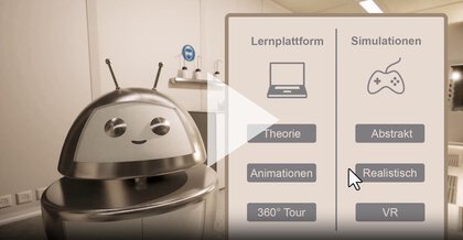
At the exhibition stand, visitors will gain insights into practical learning formats, including virtual cleanroom processes, interactive simulations, and real exhibits. VR applications illustrate the sequence of sample processes in the cleanroom. Additionally, there will be wafers in various stages of production on display, including a piezoresistive pressure sensor and 3D-printed sensor models.
Based on these, interactive simulations for a virtual technology laboratory have been developed that enable machine operation to be practiced in abstract and realistic forms. These simulations clearly illustrate how digital technologies connect research, teaching, and practice.
The goal is to impart skills to tomorrow's skilled workers in a sustainable and practical manner and thus contribute to securing a workforce in semiconductor and microsystem technology.
This special exhibition is intended for specialists and managers in semiconductor and microsystem technology, as well as for training and further education institutions, students, and young professionals. It particularly targets individuals seeking innovative qualification paths or wishing to experience technologies firsthand, such as clean room processes, simulations, and digital learning formats for securing future-oriented skilled workers.
PhoenixD Cluster of Excellence
Optical technologies are among the most important key technologies of the 21st century. From scanners at store checkouts to laser applications in the automotive industry, communications, and medicine, the technical use of light makes our digital everyday life possible.
Around 150 researchers from the fields of physics, mechanical engineering, electrical engineering, chemistry, computer science, and mathematics work together in the PhoenixD Cluster of Excellence at Leibniz University Hannover. Together, they explore opportunities for developing novel optical systems, manufacturing them, and applying them through digitalization. Partner institutions include the Technical University of Braunschweig, the Max Planck Institute for Gravitational Physics (Albert Einstein Institute), the Physikalisch-Technische Bundesanstalt, and the Laser Zentrum Hannover e.V.
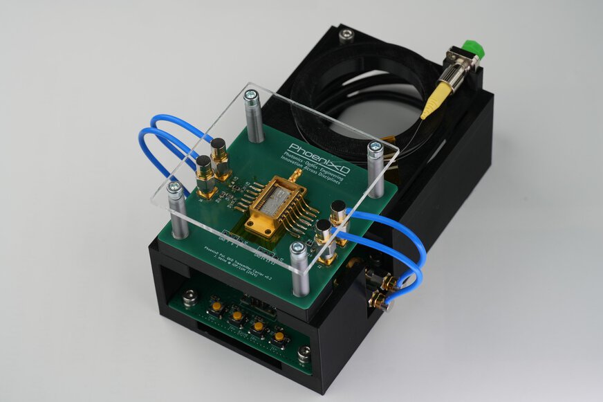
At the trade fair, the researchers will present two projects:
- A micro-optical system on a glass substrate for tap-proof telecommunications.
- An electro-optical circuit board with printed optical waveguides, which serves as an optical interface in power converters and for the galvanic, interference-free separation of circuits at different voltage levels.
The focus is on innovative manufacturing processes – such as the maskless creation of mounting openings, additively manufactured gold contacts, and the active adjustment of micro-optics during assembly. In addition, the integration of printed optical fibers into printed circuit boards and the synchronization of highly productive processes for stable system function will be demonstrated.
Both exhibits impressively demonstrate the interplay between modern production techniques and optical and quantum technologies. Visitors can test their knowledge of these future technologies at the Wheel of Fortune and discuss possible applications and collaborations with the researchers.
The target audience includes companies with expertise in the assembly or passive implementation of optical coupling that are interested in collaborating, as well as original equipment manufacturers (OEMs) who could be partners in future research projects. School pupils, students, and doctoral candidates interested in learning about courses and career opportunities at Leibniz University Hannover and the PhoenixD research cluster are also welcome.
Die Evolution der Leiterplatte – p² Pack Technologie
At the special exhibition, Schweizer Electronic AG will show what the printed circuit board of the future will look like: more powerful, compact, and efficient. With p²-Pack technology, semiconductor chips, such as silicon carbide (SiC) power semiconductors, can be embedded directly into the printed circuit board. This results in significantly lower thermal resistance, minimal inductance, and maximum power density.
The highlight is the p² Pack technology, which allows for an entirely new type of system integration. Semiconductor chips are embedded directly into the circuit board. This reduces thermal resistance and switching losses while significantly increasing power density and efficiency.
The exhibit, a starter generator from Schaeffler, demonstrates the technology's advantages in a real-world application. Importantly, the p² Pack technology is not limited to the automotive sector but can be used in numerous industrial areas that require maximum reliability, efficiency, and miniaturization. Thus, Schweizer Electronic offers a key technology for the next generation of power electronics.
This special exhibition is aimed at trade visitors from the manufacturing and industrial electronics sectors, as well as power electronics developers and decision-makers. Anyone interested in innovative PCB solutions and forward-looking packaging technologies will find it particularly interesting, whether they work in the automotive industry, industrial automation or renewable energies.
The world of autonomous driving: building trust through all the senses
The special exhibition area “The world of autonomous driving: building trust through all the senses” presents multisensory solutions that will enhance the experience and safety of future vehicles. Among other things, it will display innovative approaches to verbal interaction between humans and vehicles, AI-based methods for acoustic monitoring of vehicle condition, and solutions for interior and exterior communication. The focus is on using acoustics and sensor technology to inspire confidence in autonomous driving functions.
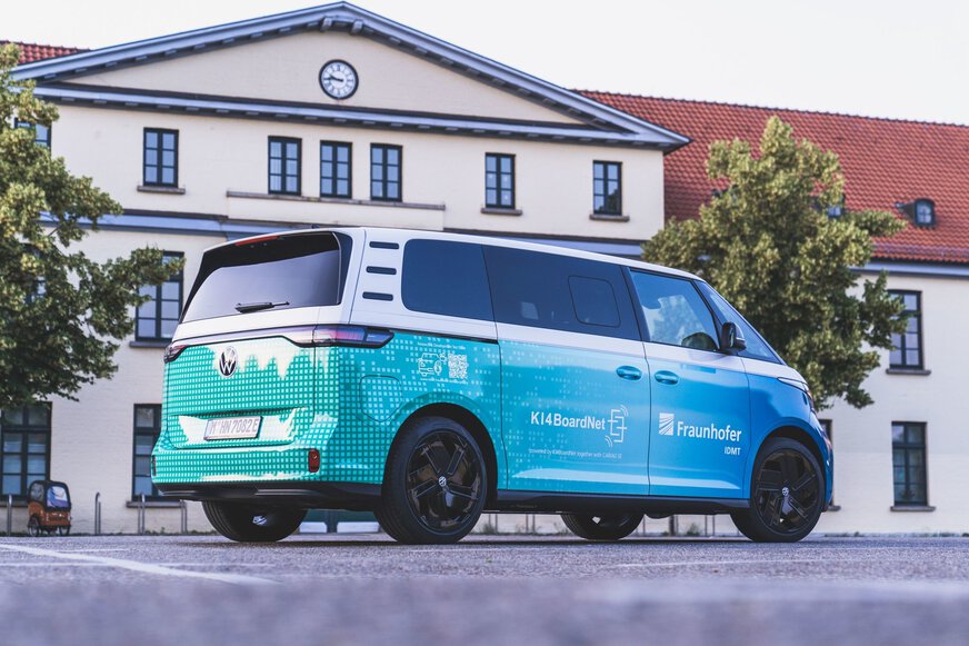
There will be exhibits that focus on the interplay between acoustics and AI. A notable exhibit is the robust speech recognition technology, which enables reliable voice control even in the presence of background noise. The holistic approach is unique: it examines all acoustic aspects, from AI-supported condition monitoring (e.g., tire pressure) to sound design for warning signals (AVAS) to communication between vehicles and pedestrians. The unique selling proposition (USP) lies in the multisensory experience of the technologies, which can be experienced live to promote trust in complex systems.
This special show primarily targets trade visitors from the automotive industry. This includes vehicle manufacturers, suppliers, technology developers, and service providers specializing in acoustics, sensor technology, AI, and human-machine interaction. The exhibition offers these experts a platform to learn about the latest research and development results.
Power, Packaging & Trusted Electronics by SAL
Silicon Austria Labs (SAL) presents industry-ready research from the wafer level to intelligent systems. SAL's unique selling point lies in its combination of application-oriented, cutting-edge research and industry-oriented pilot lines, such as the MicroFab and Packaging Labs. This allows partners to experience future technologies in a practical setting and swiftly integrate them into their products and processes.
We present highly efficient power electronics (design, control, EMC & characterization), advanced packaging & heterogeneous integration (including wafer-level, 2.5D/3D, and photonic packaging), and trustworthy microelectronics (formal verification, security including post-quantum cryptography and side-channel analysis).
In addition, we offer the topics “Advanced Sensors & Electronics Technologies,” such as printed/flexible sensor technology with chip integration, and “Microsystems Highlights,” including thin-film, piezo, and integrated photonics technologies.
At SAL MicroFab, we bridge the gap between research and pilot production. In short, SAL brings efficiency, reliability, and trustworthiness in electronics manufacturing to life—from the packaging process to the tested, verified system.
SAL demonstrates its interdisciplinary strength along the entire electronics value chain:
- Power electronics: Wide bandgap technologies, modular topologies, and optimized cooling for maximum energy efficiency.
- Advanced packaging: 2.5D/3D integration, system-in-package, wafer-level packaging, and sustainable materials for compact, robust systems.
- Trusted electronics: Security and reliability through formal verification, tamper-proof electronics, and post-quantum security.
- Advanced Sensors & Microsystems: novel sensor technologies, integrated photonics, piezoelectric actuators, and flexible electronics.
This special show is aimed at decision-makers, developers, and production managers in electronics manufacturing, mechanical engineering, the automotive industry, the energy sector, and industrial applications. These professionals are looking for innovative solutions to increase the efficiency, miniaturization, integration, and security of the next generation of electronic systems.

