Current challenges in the semiconductor industry

productronica—the world’s leading trade fair for electronics manufacturing and development—showcases the latest innovations in the microelectronics industry in Munich. The manufacture of semiconductors is a focal point of the trade fair. Visitors can gain insights about the current trends surrounding materials, packaging technologies and manufacturing processes.
Current challenges in semiconductor manufacturing
From household appliances and cars to space—countless instances of technological progress are made possible by microchips and thus semiconductor technology. For many decades, industrial countries have been in a race to produce the most powerful chips in order to gain a leading position in the microelectronics industry. However, only a few companies worldwide are capable of carrying out the complex process of manufacturing semiconductors.
This is due in part to the ever smaller structure sizes of modern semiconductor chips, which are approaching 3nm structures and thus pushing traditional electronics manufacturing to its physical limits. In addition, there are new packaging technologies such as Advanced Packaging that require great precision and thus high investments. The increasing shortage of skilled workers is also making it more difficult for companies to acquire highly qualified personnel for the respective work steps. What’s more, the geopolitical situation is creating further challenges such as supply bottlenecks and logistics problems for the microelectronics industry. Special requirements also arise in industries such as medical technology or car manufacturing due to secure microelectronics, which are intended to ensure the safety and integrity of semiconductor products in critical applications.
Semiconductor manufacturing process: complex, expensive and time-consuming
Manufacturing semiconductors is a very complex process and requires in-depth knowledge of the technology. Put simply, the production of a microchip consists of the following steps:
- Manufacturing the wafer: quartz sand, ingot, wafer
- Processing the wafer: lithography and etching
- Producing conductivity: doping, oxidizing and metallizing
- Testing, processing and packaging the semiconductor
Producing the wafer
The starting point for a microchip is quartz sand, from which high-purity silicon is extracted in several steps. A large single crystal is grown from this at temperatures of more than 1,000 °C, usually using the Czochralski process named after the inventor. The finished single crystal—also known as an ingot—is cut into thin slices (wafers). These wafers are then polished and cleaned to achieve 100 percent purity.
Processing the wafer
The actual electronic structures such as transistors are created on the wafer using a lithography process. To do this, thin layers of photoresist are applied and certain predefined patterns are exposed using photolithography. The material that is not covered by the lacquer is then removed by chemical (wet) or dry (plasma) etching. What remains is the desired structure of the wafer, which is then coated (doped) with different materials.
Establishing the conductivity
During doping, materials such as boron or phosphorus are introduced into the semiconductor material to define the conductivity of the semiconductor. The process is done by using n-, p- or pn-doping. The final steps in microchip production—which are repeated several times—are oxidation in high-temperature ovens and metallization, in which the conductor tracks are applied to the semiconductor.
Testing, processing and packaging the semiconductor
Finally, each chip is tested for full functionality to ensure that the chips meet their specification requirements. The chips are then separated from the wafer and placed on a carrier structure in the final packaging process. Extensive quality controls ensure that the chip is fully functional.
Quality control in semiconductor manufacturing
Extensive quality controls at various stages of production ensure that the finished microchips work according to their predetermined function and comply with all specifications. Artificial intelligence (AI) methods are increasingly being used here.
Inline quality control
Inline quality checks are carried out directly during the production process and are usually automated and contactless, for example using optical laser sensors that continuously check the spacing, diameter or thickness of the wafers. AI-supported camera systems can also specifically detect and report incorrect exposures, foreign particles or cracks in the material.
Testing the finished microchips
Before the individual chips—also known as dies—are separated from the wafer, they undergo an initial functional test. The manufacturer checks which dies work and which do not. For this purpose, the wafer is placed in a test device and the individual contact points are checked for functionality. For example, parameters such as leakage currents, clock frequency limits, current consumption or signal delay are tested.
Final test after packaging
Before the die can be delivered to the customer, the microchip, which has already been packaged and placed in its housing, has to undergo a final quality check under real conditions. It is controlled with real signals to check whether all inputs and outputs react correctly.
A stress test under high temperature, voltage and load ensures that failures are detected at an early stage, and limit loads at the lower end of the specification are also tested. This allows data on power consumption, clock frequency, response times and leakage currents to be recorded and evaluated.
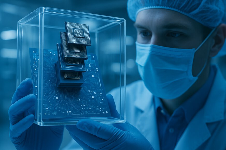
Clean-room technologies in semiconductor production
Even the smallest particles can lead to rejects and defective end products when manufacturing semiconductors. For this reason, the production process takes place in specially equipped clean rooms in which particle concentration, temperature, humidity and pressure are strictly regulated. For example, the ambient air is constantly circulated through special filter systems and employees are equipped with appropriate protective clothing. Strict access controls ensure that only people who comply with all of the necessary protective measures enter a clean room.
To meet the highest quality requirements for a clean room, there are certifications in accordance with ISO 14644-1. This defines how many particles of a certain size may be present in a cubic meter of air—the lower the class, the cleaner the room. Accordingly, a distinction is made between ISO 1—the “cleanest” air with fewer than 10 particles per cubic meter of air—and ISO 9 with more than 100 million particles per cubic meter of air.

Market forecast for the semiconductor industry
The market for the manufacture of semiconductors has experienced a variety of cuts and upheavals in recent years. For example, Taiwan now has almost 65 percent of global foundry capacity, mainly due to TSMC. Taiwan is followed by South Korea, the United States, China and Japan. Europe currently manufactures around 9 percent of the world’s semiconductors, with the largest shares coming from Germany, Ireland and France – with the aim of increasing this share to around 20 percent by 2030.
Bundled expertise at productronica and SEMICON Europa Munich
Exhibitors from across the world of electronics manufacturing at the world's leading trade fair for semiconductors productronica and SEMICON Europa, which will take place at the same time, will offer insights into how the resilience of semiconductor manufacturing can be increased. A full list of the exhibiting companies can be found in the interactive exhibitor directory.
Above all, the European Chips Act, with a total volume of EUR 43 billion, is intended to boost Europe’s semiconductor production capacities and strengthen Europe as a top region for electronics manufacturing. The EU is providing a total of around EUR 11 billion in funding for this, with the remainder coming from private and national sources. These funds will flow into research and development as well as the production of semiconductors.
Extensive activities in research & development
One important area of research is the pilot line for “Advanced Packaging and Heterogeneous Integration for Electronic Components and Systems” (APECS for short), which is being implemented as part of the EU Chip Act. It is intended to drive technological progress in the field of chiplets and increase research and production capacities for semiconductors in Europe.
One focus of APECS is quasi-monolithic integration (QMI), in which several chips are accommodated in a small space or very closely interconnected in a stack arrangement. Thus, APECS is to become Europe’s leading research hub for Advanced Packaging and play a key role in Europe’s microelectronics industry. Visitors to the world's leading trade fair productronica in Munich can be inspired by research projects such as APECS or current projects of the Fraunhofer-Gesellschaft.
What can trade fair visitors and exhibitors expect at the Semiconductors Cluster?
The Semiconductors Cluster and semiconductor technology ideally complement the associated areas of electronics manufacturing, which also include the Cables, Coils & Hybrids Cluster and SMT.
In addition to solutions for semiconductor production, the manufacture of displays, LEDs and discrete components, you will find everything about photovoltaic production, micronano production as well as material processing and clean-room technology. It is something that excites both exhibitors and trade fair visitors: With SEMICON Europa, which is once again taking place alongside productronica in Munich, the world’s leading trade fair for development and production is expanding its offering in the semiconductor industry.
Exhibitors in the Semiconductors cluster
Around 300 exhibitors from across the globe were present at the Semiconductors cluster of the trade fair in 2025. Among the companies that have already registered are Bach Resistor Ceramics, BESI BE Semiconductor Industries, BRIDGE, BUSCH Microsystems Consult, Diener electronic, F & K DELVOTEC Bondtechnik, Harms & Wende, HÜBERS Verfahrenstechnik Maschinenbau, INMATEC Gase Technologie, Kulicke & Soffa, RAMPF Holding, Universal Instruments, and Yamaha Robotics.
You can see which electronics manufacturing companies were at productronica 2025 in the interactive exhibitor directory. ( link).
The exhibition areas in the Semiconductors cluster at the trade fair are:
- Semiconductor manufacturing
- Production of displays, LEDs and discrete components
- Photovoltaic production
- Micro-/nano production / MEMS
- Clean-room technology
- Material processing
productronica supporting program on the topic of semiconductor production
In practice oriented forums, live demonstrations and various special shows, you will gain insights into the latest industry trends and challenges in the field of semiconductor production.