Advanced Packaging—New Combinations for Greater Performance and Safety
Dive into the focus topic “Advanced Packaging.” Discover how innovative technologies and novel combinations are revolutionizing the deployment and integration of semiconductors, acting as enablers for “More-than-Moore.”

The Focus Topic: Advanced Packaging
Experience how Advanced Packaging is fundamentally transforming modern electronics manufacturing. New combinations of design and production techniques are enabling more complex system integration and higher performance. They are also driving advancements in miniaturization, efficiency, reliability, and safety.
What does Advanced Packaging mean for innovation?
Advanced Packaging is a key driver of innovation in the semiconductor industry. It enables more powerful, compact, energy-efficient, and increasingly intelligent systems. Applications include:
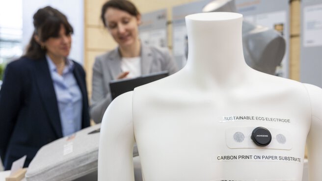
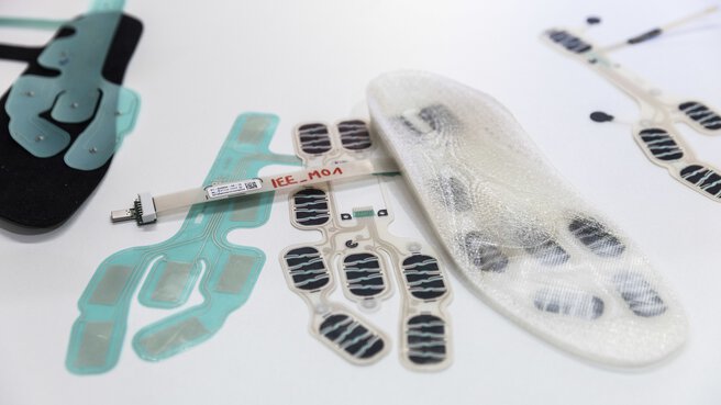
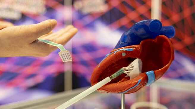
- Medical Technology: Implantable sensors and diagnostic devices with ultra-compact chiplets.
- Quantum Computing Precursor Systems: Ultra-cool, precise interfaces between control electronics and qubits.
- High-Performance Computing: 2.5D/3D packaging and interposer technologies enable extreme computing power in a compact form factor – for cloud computing or simulations.
- Automotive Industry: SiPs (System-in-Package) for radar, lidar, infotainment, and control units – now also used in ADAS systems and power modules for electric drives.
- Automation Technology: Robust SiPs for sensor fusion, edge AI, and predictive maintenance.
- Telecommunications Infrastructure: Advanced RF packaging in base stations, antenna modules, and modem chips – offering lower latency and improved signal quality.
Why is Advanced Packaging especially important right now?
- Performance Requirements: Increasing power densities, higher data rates, and lower latencies. Advanced Packaging supports these through shorter signal paths, more efficient power delivery, and improved thermal management.
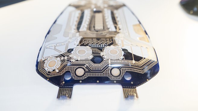
- Heterogeneous Integration: Allows different semiconductor technologies – logic, memory, RF, photonics – to be combined. The result: functionality-packed systems in minimal space with optimized performance.
- Miniaturization: Rising complexity and limited space in end devices (e.g., implants) require advanced miniaturization. Techniques like fan-out wafer-level packaging (FoWLP) and 3D chip stacking support this.
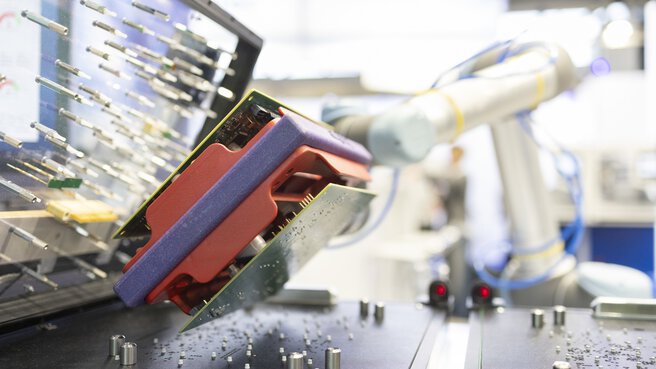
- Precision Requirements: Demands assembly accuracies in the micro- to nanometer range. High-precision placement systems, Cu-Cu bonding, and wafer-to-wafer alignment are key technologies in this area.
- Advanced Testing Strategies: Requires integrated testing from wafer to system level. Hidden faults pose a risk – design-for-testability becomes a core requirement.
- Material Innovation: New materials improve thermal properties, mechanical stability, electrical insulation, and overall reliability – crucial for modern high-performance applications.


What are the challenges in Advanced Packaging?
- Integrating various connections like flip-chip or hybrid bonding requires precise manufacturing techniques and processes.
- Mounting components at nanometer precision is highly challenging.
- Increased logistics complexity necessitates efficient data networking across the entire value chain.
- Cross-system testing strategies down to individual components are necessary – requiring additional resources and technologies.
- Innovative thermal management is essential to minimize overheating risks at higher power densities.
The trade fair program on the focus topic of Advanced Packaging
The forces shaping the Advanced Packaging sector are also highlighted in productronica’s high-profile supporting program—focusing on knowledge transfer and professional exchange.
Which companies will present their solutions and products related to Advanced Packaging?
At productronica 2025, numerous companies will showcase innovations in Advanced Packaging, including:
- Semiconductor Manufacturers: Designers and producers of complex semiconductors and chips
- Connection Technology Providers: Experts in soldering, wire bonding, flip-chip, and hybrid bonding
- Material Suppliers: Producers of specialty materials like epoxy resins or glass ceramics
- Equipment Manufacturers: Makers of machinery and equipment for production and assembly
- Quality Assurance Service Providers: Providers of specialized testing and inspection services
Which forums are dedicated specifically to this topic?
productronica 2025 will feature four forums. These will include high-level speaker presentations, inspiring workshops, and valuable discussions, also focusing on Advanced Packaging.
Exhibitors on the focus topic of Advanced Packaging
Renowned exhibitors will present the latest developments, solutions, products, and services in the field of Advanced Packaging. See which established industry leaders and up-and-coming startups will be attending productronica 2025 in the exhibitor directory, updated daily.